NVIDIA NVHBM Boosts Memory Bandwidth 30% for Custom AI Chips
NVIDIA expands NVLink Fusion with NVHBM, a custom HBM that delivers 30% more memory bandwidth and 15% lower power. Amazon's Annapurna Labs is first to adopt it.
NVIDIA has expanded its NVLink Fusion platform with NVHBM, a new high-bandwidth memory (HBM) design that moves the memory controller off the main processor die and into the HBM stack itself. The result is up to 30% more memory bandwidth, 15% lower HBM power draw, and 25% more usable compute area on the XPU die compared with standard HBM4E. Amazon's Annapurna Labs is the first partner confirmed to use the technology, with plans to integrate it into Trainium4 and future AWS AI chips.
What happened
| Metric | NVHBM vs standard HBM4E |
|---|---|
| Memory bandwidth gain | Up to 30% higher |
| HBM power reduction | Up to 15% lower |
| XPU compute die area freed | Up to 25% more |
| First adopter | Amazon Annapurna Labs (Trainium4) |
| Supplier model | Multiple memory providers, single standard spec |
NVIDIA announced NVHBM as an addition to its NVLink Fusion programme, which lets hyperscalers and chip designers connect their own custom processors to NVIDIA’s rack-scale networking and systems platform. NVLink Fusion already gives partners access to NVLink chiplets, NVLink-C2C interconnects, NVLink Switches, and NVIDIA MGX racks.
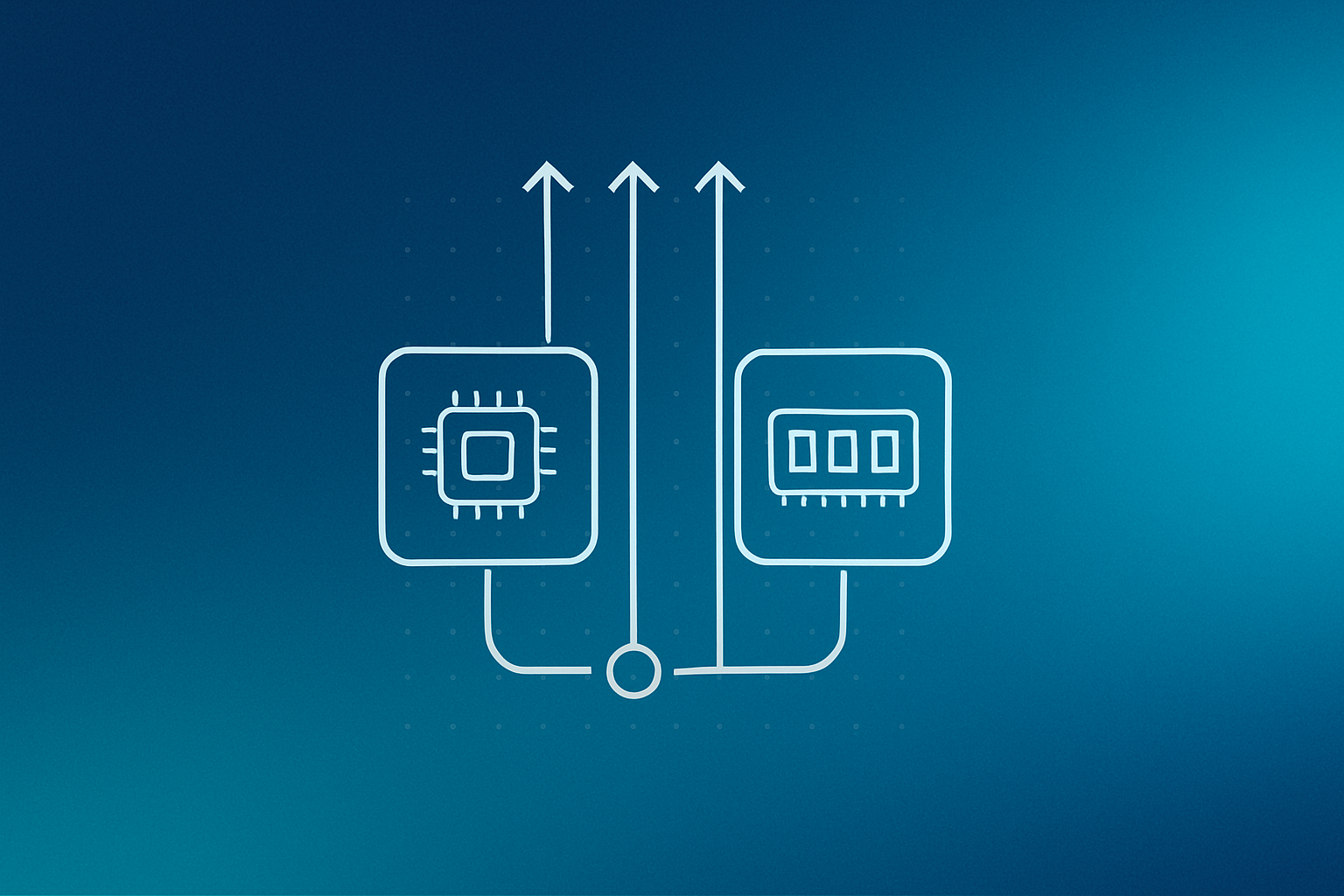
The core architectural change in NVHBM is where the memory controller lives. In conventional HBM designs, the memory controller sits on the XPU die itself, consuming silicon space that could otherwise hold compute logic. NVHBM shifts that controller into the base die of the 3D HBM stack, the same approach NVIDIA says it will use in its own future GPUs. That single change is what drives the bandwidth, power, and area improvements.
Why does the memory controller location matter?
Silicon area on a high-end AI chip is expensive and finite. Dedicating a significant portion of it to memory control circuitry is a direct cost to compute density. By relocating that logic into the memory stack, chip designers get back usable compute area without shrinking the overall package. At trillion-parameter model scales, where memory bandwidth is often the bottleneck, a 30% bandwidth uplift is a meaningful number, not a rounding error.
NVIDIA is also standardising the NVHBM implementation across multiple memory suppliers. That matters because qualifying memory from a single vendor is already time-consuming. A common specification means a chip designer validates once and can source from several suppliers, which shortens time to market and reduces supply-chain risk.
Amazon Annapurna Labs leads adoption
Nafea Bshara, VP of Annapurna Labs at Amazon, confirmed the collaboration, describing NVHBM as “a new architectural approach to advancing high-bandwidth memory performance and efficiency.” Annapurna Labs will apply the technology to its NVLink scale-up architecture work and plans to support NVLink Fusion starting with Trainium4. That chip would allow Amazon’s custom AI accelerators and NVIDIA GPUs to share a common rack-scale architecture, according to NVIDIA.
This is an extension of AWS’s previously announced NVLink Fusion support, not a new partnership from scratch. The addition of NVHBM deepens the hardware integration between the two companies’ silicon roadmaps.
For context on how major cloud providers are ramping their GPU and custom chip strategies, see our earlier coverage of Amazon tripling its Nvidia GPU order to 2 million chips for AWS.
Our take
NVHBM is a smart piece of vertical integration dressed up as an open standard. NVIDIA gets its memory controller technology embedded in every chip that joins the NVLink Fusion ecosystem, which deepens platform lock-in while genuinely delivering better hardware specs. The 30% bandwidth and 25% die-area numbers are real engineering wins that chip designers will care about.
For businesses evaluating AI infrastructure, the direct takeaway is that AWS’s Trainium chips are getting more capable and more tightly integrated with NVIDIA’s networking fabric. If you run large model training on AWS, Trainium4-based instances may offer a meaningfully different performance-to-cost profile compared with current GPU instances. Watch for Trainium4 instance announcements and benchmark them against your actual workloads before committing to a long-term cloud contract.
If you are building or scaling AI-powered products and want to understand how infrastructure choices affect cost and performance, the AI integration services we offer at Lumien can help you map the right stack for your use case.
What to do about it
- Track Trainium4 availability announcements from AWS and request early access if you run large training workloads.
- Compare memory-bandwidth-per-dollar across Trainium4, H100, and GB200 instances once benchmark data is public.
- If you are a chip designer or hardware startup, contact NVIDIA’s NVLink Fusion partner programme to understand NVHBM qualification requirements and lead times.
- For software teams, audit whether your model serving code is memory-bandwidth-bound or compute-bound. A 30% bandwidth increase only helps if your bottleneck is memory throughput.
The practical bottom line: NVHBM makes NVLink Fusion a more compelling platform for any organisation building or buying custom AI silicon, but the real impact will show up in instance pricing and benchmark sheets, not press releases.
Frequently asked questions
What is NVIDIA NVHBM?
NVHBM is NVIDIA's custom high-bandwidth memory technology that moves the memory controller from the XPU die into the base die of the 3D HBM stack. Compared with standard HBM4E, it delivers up to 30% more memory bandwidth, 15% lower HBM power consumption, and frees up to 25% more compute area on the XPU die.
What is NVLink Fusion?
NVLink Fusion is NVIDIA's programme that lets hyperscalers and chip designers connect their own custom XPUs and CPUs to NVIDIA's rack-scale platform, including NVLink chiplets, NVLink Switches, and MGX systems, without building the full networking and systems stack themselves.
Which companies are adopting NVHBM first?
Amazon's Annapurna Labs is the first confirmed partner for NVHBM, planning to use it in its Trainium4 chips as part of an expanded collaboration with NVIDIA around NVLink Fusion.
How does NVHBM compare to HBM4E?
According to NVIDIA, NVHBM delivers up to 30% greater memory bandwidth, up to 15% lower power consumption, and frees up to 25% more silicon area on the XPU compute die compared with standard HBM4E.